| |
Fundamental TechnologiesVoyager LECP Pages |
Circuit Detail
The PHA can be analyzed using the included block diagrams, timing diagrams and circuit schematics. The following comments are guides to the drawings and diagrams and include a number of unique areas encountered. A prototype tester is available with one set of the basic A/D converter and control boards. As of July 1977 no spare set of Peak Detector boards was available. The test set, test mounts and spare boards are in storage at the S1P electronics laboratory, Howard County, building 4, room 237.
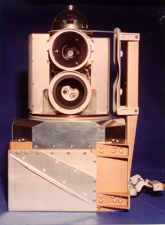
The Pulse Height Analyzer consists of 10 printed circuit boards in the Pulse Circuit Assembly of the Low Energy Charged Particle experiment. The boards include the following:
| 1520-1 | Fast Comparator and Multiplexer for the #1 PHA |
| 1520-2 | Same for the #2 PHA |
| 1530-1 | Reference Voltage and Power Switching for #1 PHA including Peak Detector power switches |
| 1530-2 | Same for the #2 PHA but does not include Peak Detector switches. Line interconnects with the 1530-1 board to accomplish Peak Detector power during PHA-2, LEPT operation. |
| 1540-1 | A/D cycle logic with R/2R ladder drivers |
| 1540-2 | Same as above for #2 PHA |
| 1550-1 | Experiment interface and standby logic. Controls timing and performs logic level shift from 8V external to 12V internal |
| 1550-2 | Same as above for #2 PHA |
| 1560 | Peak Detectors and Discriminators |
| 1570 | Buffer Amplifiers and peak detection logic control |
The 1520, 1530, 1540, and 1550 boards work together as a unit performing analog to digital conversion and multiplexing upon receipt of the experiment GO pulse. The 1560 and 1570 boards work together as five channels of peak detection with no interaction to the rest of the PHA except for power control and the HOLD function.
PHA to Experiment Interface and Control. The 1550 and 1530 boards provide power control, input line buffers, output line drivers and most of the logic necessary for the interface. The detailed block diagram of Figure 2 illustrates the power control structure wherein the major portion of the PHA circuitry stays OFF except during the analog to digital conversion cycle. Also, power to the peak detector and buffer boards (1560 and 1570) is on only when one of the A/D converters is under power and in the LEPT mode.
Power voltages are switched by either of two EME hybrids (0265 and 0274) as designed by D. Fort. These use J-FET switches to achieve efficient power control. Standby power is controlled by a type II (EME 0265) switch hybrid which is minimum power drain but slow switching. Cycled power for the A/D conversion cycle is controlled by a type III (EME-0274) hybrid and two transistors to obtain rapid turn ON (typically less than 3 microseconds) at the start of the cycle. Three types of power distribution are shown in Figure 2, the standby power as dotted voltages, conversion cycle power as "S" voltages, and peak detector circuit power as "P" voltages. In all cases the switch hybrids are turned ON by a positive voltage at the control pin.
The standby circuits of the main electronics are shown as the right hand portion of Figure 2 and are separated from the cycled power blocks by a vertical dashed line. This circuitry must accomplish the following:
PHA Standby Circuit Functions
Most of the control and interface circuitry is on the 1554 board. The schematic shows the interfaces are accomplished with hex buffers, inverters for the input control lines and non-inverters on the output digital lines. An exception is the clock detection Schmitt-trigger which is designed using three NAND gates. Schmitts were not available for this program. Logic level translation from the internal +12 to the required +8 V output is done directly by the CD4050 buffer. Input level shift from +8 to +12 is more difficult and required transistors Q1 through Q5. The transistor bias circuit for Q1 and Q5 uses a hot-carrier clamp diode (CR-1 and CR-2) to prevent saturation and maintain fast turn-off in the "Go" and "Clk" circuits. The transistor collectors have the same phase as the emitters and switch between about +0.2 V above the drive lower voltage and +12 volts. This logic voltage shaft was done in the interest of using as high a reference voltage as practical (8.000V) to minimize offset errors and noise during the analog to digital conversion.
Interface noise rejection is enhanced by the clock Schmitt-trigger and providing shaped transitions on the output lines. False clock pulses would be a major problem since they could cause internal logic state jumps and pronounced malfunction. Shaping the output transitions both reduces cross coupling in the cabling and minimizes ringing at the receiving end of the lines. The buffer inputs and outputs are all resistor isolated to prevent loading of the experiment Command and Data logic at times the PHA is turned OFF. Note the input lines do not have pull down input resistors and the board must not be operated without being connected to a tester or some other control to prevent excessive current drain in the U1 and U3 integrated circuits.
Conversion cycle control is accomplished by the binaries of the U6, U7 and U8 packages. The "Detailed Circuit Timing Diagram," Figure 5, shows most of the waveforms within the 1554 board.
Conversion Cycle Timing
During the cruise phase of the satellite mission, the peak detectors will be powered as part of the LEPT (Low Energy Particle Telescope) mode. These have their own synchronous timing as illustrated in Figure 1. The peak detectors hold the most positive voltage input since the last zero crossing of the analog channel, hesitate for 2 microseconds at the next zero crossing and reset to zero. The experiment data section has 2 microseconds to request a PHA reading by generating a "Go" pulse, after which time the PHA logic maintains the peak values for the duration of the total A/D conversion, nominally 910 microseconds. The only control circuits required for the peak detectors are the "Go" detector, "Set" binary and its "Hold" output. Reset is generated for all peak detectors by any of the five inputs making a negative going zero crossing after exceeding the threshold of its discriminator. Reset also occurs at the end of a conversion cycle when the PHA hold level returns to 0.
Return to Voyager LECP Data Analysis
Handbook Table of Contents.
Return to Fundamental Technologies Home Page.
Last modified 6/20/03, Tizby Hunt-Ward
tizby@ftecs.com